- 您现在的位置:买卖IC网 > Sheet目录3893 > PIC16F723A-I/SS (Microchip Technology)MCU PIC 7KB FLASH XLP 28-SSOP
PIC16(L)F722A/723A
DS41417B-page 206
2010-2012 Microchip Technology Inc.
23.4
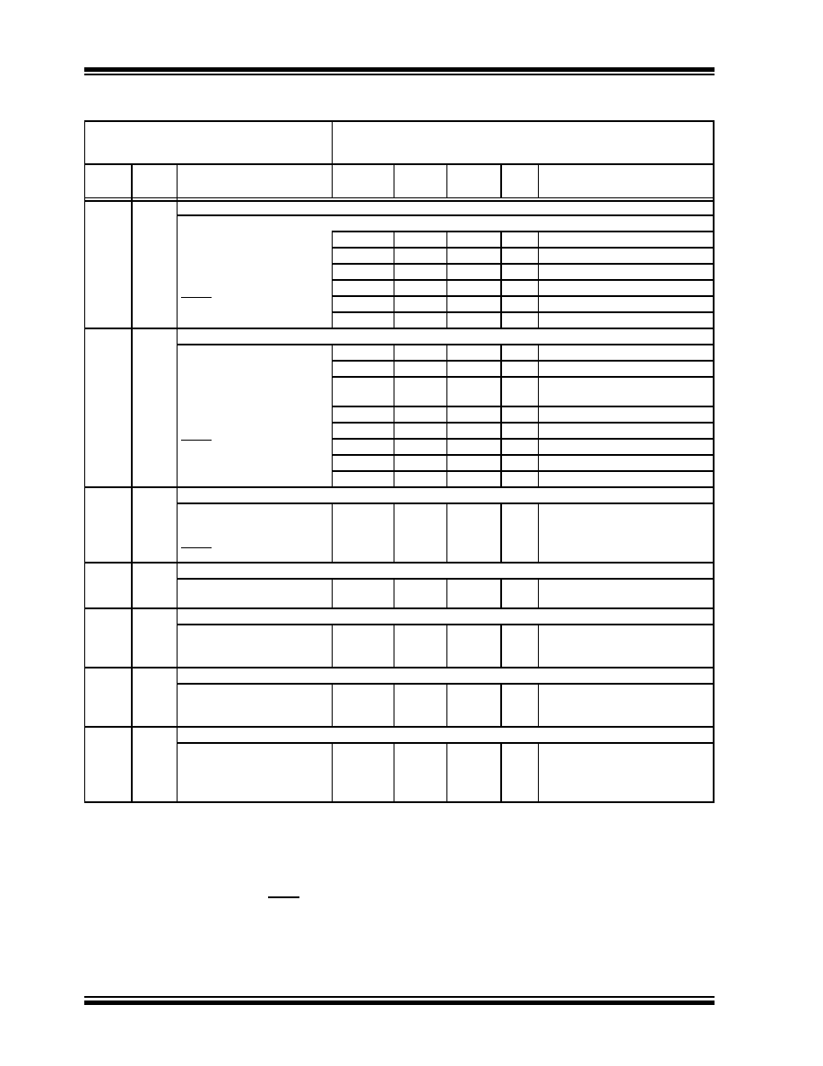
DC Characteristics: PIC16(L)F722A/723A-I/E
DC CHARACTERISTICS
Standard Operating Conditions (unless otherwise stated)
Operating temperature -40°C
TA +85°C for industrial
-40°C
TA +125°C for extended
Param
No.
Sym.
Characteristic
Min.
Typ
Max.
Units
Conditions
VIL
Input Low Voltage
I/O PORT:
D030
with TTL buffer
—
0.8
V
4.5V
VDD 5.5V
D030A
—
0.15 VDD
V1.8V
VDD 4.5V
D031
with Schmitt Trigger buffer
—
0.2 VDD
V2.0V
VDD 5.5V
with I2C levels
—
0.3 VDD
V
D032
MCLR, OSC1 (RC mode)(1)
——
0.2 VDD
V
D033A
OSC1 (HS mode)
—
0.3 VDD
V
VIH
Input High Voltage
I/O ports:
—
D040
with TTL buffer
2.0
—
V
4.5V
VDD 5.5V
D040A
0.25 VDD +
0.8
——
V
1.8V
VDD 4.5V
D041
with Schmitt Trigger buffer
0.8 VDD
——
V
2.0V
VDD 5.5V
with I2C levels
0.7 VDD
——
V
D042
MCLR
0.8 VDD
——
V
D043A
OSC1 (HS mode)
0.7 VDD
——
V
D043B
OSC1 (RC mode)
0.9 VDD
——
V
(Note 1)
IIL
Input Leakage Current(2)
D060
I/O ports
—
± 5
± 125
± 1000
nA
VSS
VPIN VDD, Pin at high-
impedance, 85°C
125°C
D061
MCLR(3)
—± 50
± 200
nA
VSS
VPIN VDD, 85°C
IPUR
PORTB Weak Pull-up Current
D070*
25
100
140
200
300
A
VDD = 3.3V, VPIN = VSS
VDD = 5.0V, VPIN = VSS
VOL
Output Low Voltage(4)
D080
I/O ports
——
0.6
V
IOL = 8 mA, VDD = 5V
IOL = 6 mA, VDD = 3.3V
IOL = 1.8 mA, VDD = 1.8V
VOH
Output High Voltage(4)
D090
I/O ports
VDD - 0.7
—
V
IOH = 3.5 mA, VDD = 5V
IOH = 3 mA, VDD = 3.3V
IOH = 1 mA, VDD = 1.8V
Capacitive Loading Specs on Output Pins
D101*
COSC2 OSC2 pin
—
15
pF
In XT, HS and LP modes when
external clock is used to drive
OSC1
D101A* CIO
All I/O pins
—
50
pF
Legend:
TBD = To Be Determined
*
These parameters are characterized but not tested.
Data in “Typ” column is at 3.0V, 25°C unless otherwise stated. These parameters are for design guidance only and are
not tested.
Note 1: In RC oscillator configuration, the OSC1/CLKIN pin is a Schmitt Trigger input. It is not recommended to use an external
clock in RC mode.
2: Negative current is defined as current sourced by the pin.
3: The leakage current on the MCLR pin is strongly dependent on the applied voltage level. The specified levels represent
normal operating conditions. Higher leakage current may be measured at different input voltages.
4: Including OSC2 in CLKOUT mode.
发布紧急采购,3分钟左右您将得到回复。
相关PDF资料
PIC12C508A-04/SN
IC MCU OTP 512X12 8SOIC
PIC12C509A-04/SM
IC MCU OTP 1KX12 8-SOIJ
PIC16LF627T-04I/SO
IC MCU FLASH 1KX14 COMP 18SOIC
PIC12C509A-04/P
IC MCU OTP 1KX12 8DIP
PIC18LC452T-I/PT
IC MCU OTP 16KX16 A/D 44TQFP
PIC12LF1822-I/MF
IC MCU 8BIT FLASH 8DFN
PIC12F1822-I/P
IC MCU 8BIT FLASH 8PDIP
PIC12F1822-I/MF
IC MCU 8BIT FLASH 8DFN
相关代理商/技术参数
PIC16F723AT-I/ML
功能描述:8位微控制器 -MCU 7KB Flash 1.8V-5.5V. 16 MHz int Osc RoHS:否 制造商:Silicon Labs 核心:8051 处理器系列:C8051F39x 数据总线宽度:8 bit 最大时钟频率:50 MHz 程序存储器大小:16 KB 数据 RAM 大小:1 KB 片上 ADC:Yes 工作电源电压:1.8 V to 3.6 V 工作温度范围:- 40 C to + 105 C 封装 / 箱体:QFN-20 安装风格:SMD/SMT
PIC16F723AT-I/MV
功能描述:8位微控制器 -MCU 7KB Flash 1.8V-5.5V. 16 MHz int Osc RoHS:否 制造商:Silicon Labs 核心:8051 处理器系列:C8051F39x 数据总线宽度:8 bit 最大时钟频率:50 MHz 程序存储器大小:16 KB 数据 RAM 大小:1 KB 片上 ADC:Yes 工作电源电压:1.8 V to 3.6 V 工作温度范围:- 40 C to + 105 C 封装 / 箱体:QFN-20 安装风格:SMD/SMT
PIC16F723AT-I/SO
功能描述:8位微控制器 -MCU 7KB Flash 1.8V-5.5V. 16 MHz int Osc RoHS:否 制造商:Silicon Labs 核心:8051 处理器系列:C8051F39x 数据总线宽度:8 bit 最大时钟频率:50 MHz 程序存储器大小:16 KB 数据 RAM 大小:1 KB 片上 ADC:Yes 工作电源电压:1.8 V to 3.6 V 工作温度范围:- 40 C to + 105 C 封装 / 箱体:QFN-20 安装风格:SMD/SMT
PIC16F723AT-I/SS
功能描述:8位微控制器 -MCU 7KB Flash 1.8V-5.5V. 16 MHz int Osc RoHS:否 制造商:Silicon Labs 核心:8051 处理器系列:C8051F39x 数据总线宽度:8 bit 最大时钟频率:50 MHz 程序存储器大小:16 KB 数据 RAM 大小:1 KB 片上 ADC:Yes 工作电源电压:1.8 V to 3.6 V 工作温度范围:- 40 C to + 105 C 封装 / 箱体:QFN-20 安装风格:SMD/SMT
PIC16F723-E/ML
功能描述:8位微控制器 -MCU 7 KB Flash 18V-55V 16 MHz Int Osc RoHS:否 制造商:Silicon Labs 核心:8051 处理器系列:C8051F39x 数据总线宽度:8 bit 最大时钟频率:50 MHz 程序存储器大小:16 KB 数据 RAM 大小:1 KB 片上 ADC:Yes 工作电源电压:1.8 V to 3.6 V 工作温度范围:- 40 C to + 105 C 封装 / 箱体:QFN-20 安装风格:SMD/SMT
PIC16F723-E/MV
功能描述:8位微控制器 -MCU 7KB Flash 1.8V-5.5V RoHS:否 制造商:Silicon Labs 核心:8051 处理器系列:C8051F39x 数据总线宽度:8 bit 最大时钟频率:50 MHz 程序存储器大小:16 KB 数据 RAM 大小:1 KB 片上 ADC:Yes 工作电源电压:1.8 V to 3.6 V 工作温度范围:- 40 C to + 105 C 封装 / 箱体:QFN-20 安装风格:SMD/SMT
PIC16F723-E/SO
功能描述:8位微控制器 -MCU 7 KB Flash 18V-55V 16 MHz Int Osc RoHS:否 制造商:Silicon Labs 核心:8051 处理器系列:C8051F39x 数据总线宽度:8 bit 最大时钟频率:50 MHz 程序存储器大小:16 KB 数据 RAM 大小:1 KB 片上 ADC:Yes 工作电源电压:1.8 V to 3.6 V 工作温度范围:- 40 C to + 105 C 封装 / 箱体:QFN-20 安装风格:SMD/SMT
PIC16F723-E/SP
功能描述:8位微控制器 -MCU 7 KB Flash 18V-55V 16 MHz Int Osc RoHS:否 制造商:Silicon Labs 核心:8051 处理器系列:C8051F39x 数据总线宽度:8 bit 最大时钟频率:50 MHz 程序存储器大小:16 KB 数据 RAM 大小:1 KB 片上 ADC:Yes 工作电源电压:1.8 V to 3.6 V 工作温度范围:- 40 C to + 105 C 封装 / 箱体:QFN-20 安装风格:SMD/SMT